
Printed circuit board Manufacturers
Keetronics ( India ) Pvt. Ltd. is a PCB design company and PCB Manufacturers in india over 30 years experience in PCB (Printed Circuit board) Industry.
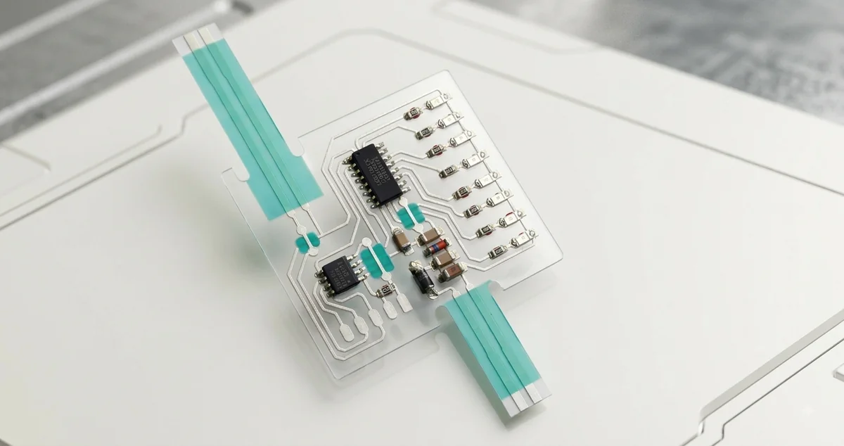
Keetronics ( India ) Pvt. Ltd. is a leading PCB Design services provider to all Reputed electronics organizations and PSU organization Globally since its incorporation. Argus Technologies offers PCB Engineering solutions like PCB Design,PCB Fabrication,PCB Assembly PCB Manufacturing, SI and Thermal Analysis,Embedded software and Hardware services,Reverse Engineering,We offer full turnkey PCB Assembly services which includes PCB Fab,Component Procurement and PCB Assembly.
Printed circuit boards (PCBs) are the foundational building blocks of modern electronics, providing both the mechanical structure to hold components and the electrical pathways to connect them.
Types of Printed Circuit Boards
-
Single-Sided PCBs: Contain a single layer of conductive material (usually copper) on one substrate layer. Used in low-cost, simple electronics like calculators and power supplies.
-
Double-Sided PCBs: Feature conductive copper layers on both top and bottom sides, connected via plated through-holes. Standard for mid-level consumer electronics and power equipment.
-
Multilayer PCBs: Consist of three or more conductive layers separated by insulating material (Prepreg/FR-4). Essential for high-density, complex devices like smartphones, laptops, and server hardware.
-
Rigid PCBs: Made from solid, non-flexible substrates like FR-4 (fiberglass). Highly durable and widely used across all major industries.
-
Flex PCBs: Built on flexible plastic substrates (like polyimide) that allow the circuit to bend, twist, or fold into compact spaces.
-
Rigid-Flex PCBs: Hybrid boards combining rigid and flexible circuit segments into a single unit, common in aerospace, medical equipment, and wearable technology.
Core Substrate Materials
-
FR-4: The industry-standard woven fiberglass and epoxy substrate offering high mechanical strength and good electrical insulation.
-
Polyimide: Highly flexible and heat-resistant polymer used in flexible PCB manufacturing.
-
Aluminum / Metal Core (MCPCB): Feature a metal base to distribute and dissipate heat rapidly, crucial for high-power LED lighting and automotive electronics.
Key PCB Assembly Techniques
-
Through-Hole Technology (THT): Component leads are inserted into drilled holes and soldered. Offers high mechanical strength for connectors and heavy components.
-
Surface-Mount Technology (SMT): Components are mounted directly onto pads on the board's surface, enabling smaller form factors and automated high-speed assembly.
The PCB manufacturing process transforms circuit designs into physical, functional electronics through a series of chemical, mechanical, and optical steps.
1. Design & Pre-Production (CAM/GERBER)
-
Design Output: Engineers generate Gerber files and drill data specifying copper layer layouts, hole locations, and component placements.
-
Design for Manufacturability (DFM) Check: The board layout is analyzed for trace spacing, drill tolerances, and potential short circuits before fabrication starts.
2. Core Fabrication & Substrate Preparation
-
Lamination & Cleaning: Core substrate material (typically FR-4 fiberglass coated with copper foil on both sides) is cleaned and prepared.
-
Photoresist Application: A light-sensitive film (dry film photoresist) is applied over the copper layers.
3. Circuit Patterning & Etching
-
UV Exposure: Circuit patterns are aligned using optical film and exposed to ultraviolet light, hardening the resist over the intended copper traces.
-
Etching: Unwanted, unexposed copper is chemically washed away using an acid solution (e.g., ferric chloride or cupric chloride), leaving behind the protected copper tracks.
4. Layer Lamination (Multilayer Boards)
-
Inner Layer Inspection: Optical cameras (AOI) scan inner layers for defects before assembly.
-
Pressing: Inner layers are stacked with epoxy-impregnated fiberglass (Prepreg) and outer copper sheets, then fused together under high pressure and heat.
5. Drilling & Plating
-
NC Drilling: High-precision computer-controlled drills create registration holes, mounting points, and component vias through the stack.
-
Electroless Copper Deposition: A micro-thin layer of conductive copper is chemically deposited inside the drilled holes to create electrical connections between board layers.
6. Outer Layer Processing & Solder Mask
-
Outer Etching & Plating: Outer copper features are plated and etched to finalize surface traces.
-
Solder Mask Application: A green, black, blue, or red epoxy coating is applied to protect copper traces from oxidation and prevent solder bridging during assembly.
-
Silkscreen / Legend Printing: Inkjet or screen printing applies component indicators, logos, and reference designators onto the board surface.
7. Surface Finish & Quality Testing
-
Surface Coating: Exposed copper pads are treated with protective finishes like ENIG (Electroless Nickel Immersion Gold), HASL (Hot Air Solder Leveling), or OSP (Organic Solderability Preservative) to prepare them for soldering.
-
Electrical Testing: E-test probe machines verify continuity (no open circuits) and test for short circuits.
-
Profiling & Routing: Individual boards are cut out from the master panel using CNC routers or laser cutting.
Key Benefits of Printed Circuit Boards
-
Compact Form Factor & High Density: Interconnections are etched onto thin conductive layers, allowing complex circuits with hundreds of miniature components to fit into extremely tight spaces.
-
Consistency & High Reproducibility: Automated manufacturing ensures that every PCB produced from a master layout has identical electrical characteristics, minimizing design variations across mass production.
-
Enhanced Electrical Performance & Signal Integrity: Fixed routing tracks reduce stray capacitance, electromagnetic interference (EMI), and signal crosstalk, ensuring stable high-frequency performance.
-
Vibration & Mechanical Stability: Surface-mounted and through-hole components are soldered securely to the substrate, preventing loose connections or short circuits caused by physical shock, movement, or heavy vibration.
-
Ease of Maintenance & Troubleshooting: Clear component placement and standardized layouts make diagnostic testing, component replacement, and field repairs straightforward.
-
Cost-Effective Mass Production: While initial design and tooling require setup, automated assembly techniques (like SMT) drastically reduce labor costs and production time for large volumes.
-
Low Circuit Noise: Carefully planned ground planes and trace geometry minimize electrical noise, improving general power distribution and circuit efficiency.
Keetronics (India) Pvt. Ltd. is specializing in custom Printed circuit board for over 30 years.
