
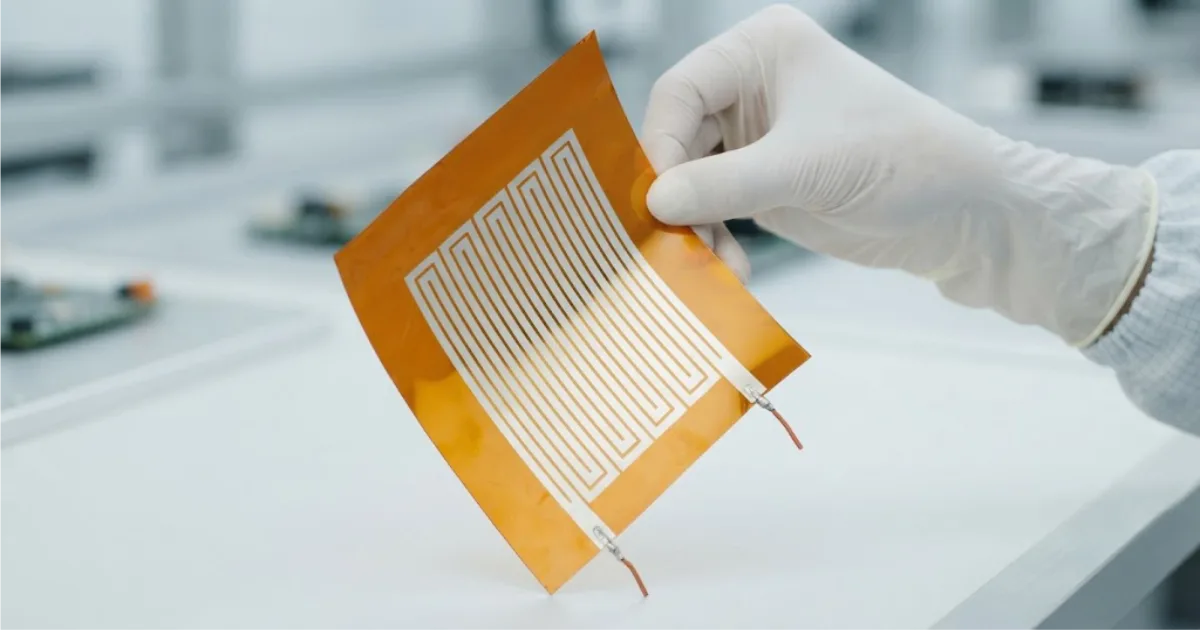
Printed Circuit Solutions can refer to two different things depending on the context: it is either a general term for professional electronics engineering services, or it refers to specific companies in the industry.
A printed circuit board (PCB) is the foundational platform used to mechanically support and electrically connect electronic components. It consists of an insulating substrate (like fiberglass) with conductive copper pathways (traces) etched onto it, which replace traditional wires to route power and signals between parts.
1. General Industry Term (PCB Services)
In the electronics industry, "Printed Circuit Solutions" refers to end-to-end services provided by manufacturers to help design, build, and assemble Printed Circuit Boards (PCBs). PCBs are the green boards found inside almost all electronic devices (like smartphones, laptops, and cars) that mechanically support and electrically connect electronic components.
These comprehensive solutions typically include:
-
PCB Design & Layout: Turning an electronic schematic into a physical board blueprint using specialized software.
-
PCB Fabrication: Manufacturing the bare boards by layering insulating materials (like FR-4 fiberglass) and etching conductive copper pathways (traces).
-
PCB Assembly (PCBA): Soldering components (like resistors, capacitors, and microchips) onto the bare board using techniques like Surface-mount technology (SMT) or Through-hole technology.
-
Prototyping & Testing: Creating rapid, low-volume test runs to validate that the circuit functions correctly before mass production.
2. Specific Company Names
Because it is a highly descriptive term, several engineering and manufacturing companies use it as their official business name. For example:
-
Printed Circuit Solutions, Inc. (PCSI): A long-standing PCB designer and quick-turn manufacturer located in California.
-
Various Global Suppliers: Many manufacturers use "Printed Circuit Board Solutions" in their branding to signal that they offer full-service manufacturing, component sourcing, and laboratory testing rather than just raw board printing.
When discussing the features of a Printed Circuit Board (PCB), we look at both its structural anatomy and its functional capabilities. Modern PCBs are highly engineered platforms designed to make electronics smaller, faster, and more reliable.
Here are the key features of a printed circuit, categorized by their structure and design:
1. Structural Elements
A bare printed circuit board is a sandwich of different material layers:
-
Substrate (Core): The base material that provides mechanical rigidity. The most common material is FR-4 (a flame-retardant fiberglass composite), though flexible circuits use Polyimide.
-
Copper Traces: The "wires" of the board. These are thin conductive pathways etched from copper sheets that route electrical signals and power between components.
-
Solder Mask: The protective layer (usually green, but can be blue, black, or white) coated over the copper. It prevents accidental short-circuits, shields against corrosion, and ensures solder only sticks where it is supposed to.
-
Silkscreen: The printed text layer (usually white) that adds labels, logos, part numbers, and component outlines to help engineers during assembly and troubleshooting.
2. Interconnection Features
Because circuits often have multiple layers of overlapping copper traces, they need features to jump between layers:
-
Vias: Tiny, copper-plated holes drilled through the board that act as vertical electrical tunnels to connect different circuit layers.
-
Through-hole Vias: Go completely through the board.
-
Blind Vias: Connect an outer layer to an inner layer but don't go all the way through.
-
Buried Vias: Connect internal layers together, completely hidden from the outside.
-
-
Pads and Lands: The exposed copper areas where component leads are physically soldered to the board.
3. Functional & Design Features
Depending on the application, PCBs are engineered with specific functional characteristics:
| Feature | Description | Common Use Case |
| Layer Count | Can range from 1 layer (simple toys) to over 30 layers (servers and supercomputers) to pack complex wiring into tiny spaces. | Smartphones, Motherboards |
| Rigid-Flex Hybridization | Combining stiff sections with flexible, bendable ribbons to fit inside oddly shaped enclosures without bulky wires. | Smartwatches, Aerospace |
| Controlled Impedance | Matching the physical dimensions of the traces to the electrical signals to prevent signal degradation at incredibly high speeds. | 5G antennas, High-speed RAM |
| Thermal Management | Integrating aluminum cores (Metal Core PCBs) or "thermal vias" to sink heat away from high-power parts. | LED lighting, Electric Vehicles |
4. Component Mounting Styles
PCBs feature two primary ways to attach components:
-
Through-Hole Technology (THT): Component pins go through drilled holes and are soldered on the opposite side. This provides strong mechanical bonds, perfect for heavy parts like connectors and transformers.
-
Surface-Mount Technology (SMT): Components are soldered directly onto the surface pads of the board. This allows components to be incredibly small and mounted on both sides of the board, maximizing space efficiency.
Transitioning from traditional point-to-point hand wiring to modern Printed Circuit Boards (PCBs) revolutionized the electronics industry.
The primary benefits of using printed circuits include:
1. Mass Production and Cost Efficiency
-
Automated Assembly: PCBs are designed for machine assembly. High-speed pick-and-place robots can populate thousands of components onto a board in minutes, drastically reducing labor costs.
-
Consistency at Scale: Once a PCB design is finalized, thousands or millions of identical boards can be printed with total precision. Every single board will have the exact same circuit layout, eliminating human error during manufacturing.
2. Compact and Lightweight Design
-
Space Optimization: Copper traces on a PCB can be etched to be as thin as a fraction of a millimeter. By stacking these traces into multiple internal layers, complex wiring that would normally take up an entire room can be condensed into something that fits inside a smartphone.
-
No Bulky Wires: Eliminating traditional insulated wires drastically reduces the overall weight and volume of an electronic device.
3. High Reliability and Durability
-
Immunity to Vibration: Because all components are soldered directly to the board's surface, they remain locked in place. This makes PCBs highly resistant to movement, drop impacts, and harsh vibrations—which is critical for automotive, aerospace, and military applications.
-
Fewer Short Circuits: Traditional wiring can fray, bend, or touch accidentally over time, leading to short circuits. A PCB's copper traces are permanently embedded into an insulating substrate and protected by a solder mask, virtually eliminating these risks.
Summary of Benefits
| Benefit | Traditional Wiring | Printed Circuits (PCBs) |
| Assembly Speed | Slow (Hand-soldered wire by wire) | Extremely Fast (Automated SMT machine) |
| Error Rate | High (Human wiring mistakes) | Low (Exact replication of a digital design) |
| Troubleshooting | Difficult (Tangled mess of wires) | Easy (Clear paths and printed silkscreen labels) |
| Electrical Noise | High (Cross-talk between loose wires) | Low (Optimized, shielded trace routi |
4. Low Electrical Noise and High Performance
At high frequencies (like in 5G, Wi-Fi, or computer processors), loose wires act like antennas, creating electromagnetic interference (EMI) and signal degradation. PCBs allow engineers to meticulously calculate trace spacing and ground planes to minimize electrical noise and ensure high-speed data transfers remain perfectly clean.
Need a custom HMI architecture for harsh operating conditions?
Talk to Our Team